
The M.Tech. VLSI program offers a comprehensive curriculum designed to equip students with in-depth knowledge and hands-on experience in the design, analysis, and implementation of Very Large Scale Integration (VLSI) systems. This program emphasizes core topics such as digital and analog circuit design, CMOS technology, semiconductor device modelling, system-on-chip (SoC) architectures, and advanced signal processing techniques. Students are trained to use state-of-the-art Electronic Design Automation (EDA) tools for creating innovative solutions tailored to the needs of various industries.
The program integrates research-driven projects, enabling students to address real-world challenges in areas like low-power design, hardware security, approximate computing, and emerging memory technologies. Students also benefit from exceptional placement and internship opportunities with leading companies such as Synopsys, AMD, Intel, and Microchip, which further enhance their industry readiness. International program opportunities allow students to collaborate with global universities and organizations, enriching their research experience and broadening career prospects.
The department has dedicated VLSI labs facilitated with the following:

Amrita Vishwa Vidyapeetham has not appointed any Agent or Third-Party Client for securing admission in any programme. Students are hereby requested to contact only the toll-free number on our website for any admission related queries.
For International Admissions, the University may work with authorized overseas representatives in select countries. International applicants are advised to verify the credentials of such representatives through official Amrita communication channels before proceeding with applications or payments.
– Issued in Public Interest by Directorate of Admissions and Academic Outreach

Two years
| Type | Code | Course Name | Teaching Schemes | Credits | ||
| L | T | P | ||||
| FC | 25VL601 | Semiconductor Device Modelling | 3 | 0 | 0 | 3 |
| SC | 25VL602 | CMOS Digital Integrated Circuits | 3 | 0 | 0 | 3 |
| SC | 25VL603 | Digital Circuits and Systems | 3 | 0 | 0 | 3 |
| SC | 25VL604 | Analog VLSI Circuits | 3 | 0 | 0 | 3 |
| SC | 25VL605 | Computer Aided Design for VLSI Circuits | 3 | 0 | 0 | 3 |
| SC | 25VL681 | Analog VLSI and device modelling Lab | 0 | 0 | 3 | 1 |
| SC | 25VL682 | RTL design and FPGA Synthesis Lab | 0 | 0 | 3 | 1 |
| HU | 22ADM501 | Glimpses of Indian Culture | 0 | 0 | 3 | P/F |
| HU | 23HU601 | Career Competency- I | 0 | 0 | 3 | P/F |
| HU | 25AVP501 | Mastery Over Mind (MAOM) | 1 | 0 | 2 | 2 |
| Total | 16 | 0 | 11 | 19 | ||
| Type | Code | Course Name | Teaching Schemes | Credits | ||
| L | T | P | ||||
| SC | 25VL611 | Functional Verification with Hardware Description Languages | 3 | 0 | 0 | 3 |
| SC | 25VL612 | Digital VLSI Testing & Testability | 3 | 0 | 2 | 4 |
| E | Elective I | 3 | 0 | 0 | 3 | |
| E | Elective II | 3 | 0 | 0 | 3 | |
| E | Elective III | 3 | 0 | 0 | 3 | |
| SC | 25VL683 | ASIC front end and back-end Design Lab | 0 | 0 | 3 | 1 |
| SC | 25VL684 | Functional Verification Lab | 0 | 0 | 3 | 1 |
| SC | 25RM604 | Research Methodology | 2 | 0 | 0 | 2 |
| HU | 23HU611 | Career Competency – II | 0 | 0 | 3 | 1 |
| SC | 25VL698 | Industry Internship* | 0 | 0 | 2 | 1 |
| Total | 17 | 0 | 13 | 22 | ||
*The internship will be during the break between the second and third semesters. This will be evaluated based on a viva-voce and a written report.
| Type | Code | Course Name | Teaching Schemes | Credits | ||
| L | T | P | ||||
| P | 25VL798 | Dissertation- Phase I | 0 | 0 | 30 | 10 |
| Total | 0 | 0 | 30 | 10 | ||
| Type | Code | Course Name | Teaching Schemes | Credits | ||
| L | T | P | ||||
| P | 25VL799 | Dissertation – Phase II | 0 | 0 | 45 | 15 |
| Total | 0 | 0 | 45 | 15 | ||
Total Credits: 66
Front End Design and Verification
*Subject to Approval
Very Large Scale Integrated (VLSI) Circuit Design is the process of designing a large computer chip (more specifically, an integrated circuit, or IC), using computer-aided design (CAD) tools on a workstation or a personal computer (PC). The course demands learning the principles of VLSI design, designing and fabricating state of-the-art VLSI chips, understanding the complete design flow and expertise to design CMOS chips for industrial requirements. The curriculum focuses on employing hierarchical design methods and understanding the design issues at the various levels of hierarchy. Students are exposed to various design softwares in this programme. Also, they learn to design, simulate, implement and test complex digital systems using FPGAs (Field Programmable Gate Arrays). The main objectives of this course are to analyze the electrical and design characteristics of transistors and gates and to study the issues and methodologies involved in the integration of these devices into complex high-performance systems.
With the recent and rapid upsurge in the areas like hardware software co-design, architectures for machine intelligence, network on chip etc. the programme is designed to cater to the needs in producing engineers trained in both hardware and software areas, bridging the gap between academia and industry. Students will be trained in several topics that cut across different domains, starting from the lowermost level of physical devices to the top level of application development.
| PO1 | Anability to independently carry out research/investigation and development work to solve practical problems. |
| PO2 | Anability to write and present a substantial technical report/document. |
| PO3 | Anability to demonstrate a degree of mastery over the area as per the specialization of the program. |
| PO4 | Ability to demonstrate deep understanding of the principles, theories, and methodologies in VLSI Design, leading to specializations in Front-end design, Verification, Back-end design, Fabrication, and Advanced Architectures. |
| PO5 | Anability to use modern tools to solve complex problems in design, development, and implementation of VLSI systems. |
| PO6 | Anability to engage in independent and life-long learning in the context of technological change and industrial demands in VLSI Design. |
*Subject to Approval
There are many options for research since VLSI design is a vast and diverse filed with front end and back end design, analog and digital domains etc. A researcher can pick and choose a specific research topic and do research in that topic. Since VLSI devices are all pervasive and ubiquitous the developments are very rapid in terms of technologies and design and there is unlimited scope for advanced research in several areas. Understanding the design flow, tools and technologies will help in choosing the right research topic. Doing a thorough literature survey on that topic will help in identifying the research gap to be filled in to solve a research problem.
With a large number of VLSI design houses in India and especially in Bengaluru, Hyderabad, Delhi etc. both as part of big global corporates (Intel, Broadcom, Qualcomm, NXP, TI, ARM, AMD, Maxim, Synopsys, Cadence, mentor Graphics, Xilinx etc.) and Indian design teams (Wipro, Waferspace, Vayuvyalabs, Mistral,Mindtree, Tessolveand many others), there is a wide scope for VLSI engineers getting placed through internships and also directly after post-graduation
Possible International Collaborations (International Universities to Pursue Dual Degree/Higher Education)
Since VLSI design is a very dynamic domain with advances happening continuously and it is the research which drives the advancements, universities are at the forefront of VLSI research. Many of the students do research leading to PhD in international universities with which collaborations are established by Amrita centre for International programmes (ACIP).
Thrust Areas in Research
Related Thrust Area Groups
Oppotunities for M.Tech VLSI Students
Ph.D. Program and Area of Focus:
Research Conducted at the Department
Apart from papers in scopus journals and conferences our top publications include IEEE Transactions in VLSI Society, Elsevier and springer
The following students joined Amrita for PhD
Amrita Vishwa Vidyapeetham is one of the top private universities in India offering a 2-year M.Tech in VLSI Design at its Amritapuri, Bengaluru, and Coimbatore campuses.
This multi-campus, prestigious academic institution offers multi-disciplinary, research-intensive courses across Engineering, Management, and Medical Sciences, including Ayurveda, Life Sciences, Physical Sciences, Agriculture Sciences, Arts & Humanities, and Social & Behavioural Sciences.
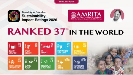
Amrita has emerged as the seventh-best university in the National Institutional Ranking Framework (NIRF) Rankings 2023 and is accredited with the highest possible ‘A++’ grade by NAAC.
With more than 250 UG, PG, and Ph.D. courses, Amrita campuses imbibe value-based education to a vibrant student population of over 24,000, helmed by 1700+ strong faculty.
One of the top institutions for higher learning, Amrita has established 180+ collaborations with the top 500 world-ranked universities and is the first choice for corporate conglomerates in India and abroad for campus recruitment.
M.Tech graduates in VLSI design typically pursue roles such as VLSI Design Engineer, ASIC Design Engineer, FPGA Engineer, Verification Engineer, Physical Design Engineer, and System-on-Chip (SoC) Engineer. These roles involve designing, testing, and implementing integrated circuits, chips, and semiconductor devices for various applications in electronics, telecommunications, automotive, and healthcare.
The salary for VLSI engineers tends to be competitive and often higher than that of average engineering disciplines due to the specialized nature of the field and the demand for skilled professionals. On average, VLSI engineers can expect starting salaries ranging from 15 Lakhs to 24 Lakhs per annum, with opportunities for significant growth with experience and expertise.
Success in VLSI design requires a combination of technical and soft skills. Technical skills include proficiency in digital design, Verilog/VHDL programming, ASIC/FPGA design flow, and familiarity with EDA (Electronic Design Automation) tools. Soft skills such as problem-solving, teamwork, communication, and project management are crucial for collaborating with cross-functional teams and efficiently delivering projects.
Yes, several industries and sectors are experiencing high demand for VLSI engineers. These include the VLSI and semiconductor industry, embedded systems, automobiles, cybersecurity, telecommunications, consumer electronics, healthcare, and aerospace. Industries undergoing rapid technological advancements and relying on electronic systems for innovation and efficiency offer promising career opportunities for VLSI engineers.
Pursuing a Ph.D. after M.Tech in VLSI design can significantly enhance career prospects by providing more profound knowledge, research experience, and specialization in specific areas of VLSI design. A Ph.D. opens doors to advanced research positions in academia, research institutions, and industry R&D divisions. It also qualifies individuals for leadership roles, consulting opportunities, and entrepreneurship ventures, contributing to personal growth and advancements in the field.
Biomedical Instrumentation lab provides a platform for students and research scholars to explore on the various equipment and software tools for the design and analysis of analog circuits.
Lab Facilities
Faculty In-charge : Dr. Madhu Mohan N
Technical Staff : Mr. S. Velmurugan
Lab Facilities
Faculty In-charge : Dr. Kirthiga S
Technical staff : Mr. K. Arulvadivel
Hardware Resources:
Industry Standard Tools:
Faculty In-charge : Mr. Mohankumar N.
Technical staff : Mr. P Raja


The top reasons to choose Amrita for your career


“The M.Tech VLSI Design program has helped me build strong fundamentals in digital design, verification, and RTL development. The in depth project research and coursework played a major role in shaping my confidence and career direction in semiconductor design.”

“M.Tech in VLSI Design for me was a dream of unknown roads and destinations with a lone aim of just achieving it all in the field. The course and guidance here aided and showed the different paths that could be available and chosen for me to get what I truly aimed and aspired for. The knowledge and experience I gained here will stay with me throughout my career.”

I successfully graduated from Amrita in 2011, earning a Master of Technology degree in Very-Large-Scale Integration (VLSI) Design. The strong curriculum paved me to earn a core job.

Amrita University’s Coimbatore campus M.Tech program in VLSI Design was a game-changer for my career. The comprehensive curriculum and practical training equipped me with cutting-edge skills.

The diverse range of industrial-oriented subjects has provided me with a robust foundation in VLSI design, equipping me with the skills needed in today’s competitive landscape. . The exposure and skills gained during the course have proven invaluable in my professional journey.

I feel grateful for being a part of Amrita University, Coimbatore campus which helped me learn new concepts and empowered me to pursue my dreams and achieve success in my career. Throughout my academic journey, I was impressed by the faculty’s dedication and willingness to support and encourage students.

The journey through Amrita helped me to grow personally and professionally. The professors and the staff here are supportive and approachable.

Graduating with M-Tech VLSI Design from Amrita University, Coimbatore campus was one of the best decisions of my life. The 2-year intensive program has helped me to advance my knowledge.

The curriculum of all the subjects in the discipline was up to date with current industry standards. Labs were equipped with sufficient tools. Placement cell helped us get an internship opportunity by bringing in several product companies.

As we all know , Amrita Bangalore Campus is a renowned educational institution offering quality education and producing graduates who compete and excel on both national and international levels. Studying M-Tech here was one of best decision of my life, college have well experienced teaching faculty, they guided our batch such that all of my classmates including me , got placed in Top multinational companies. With the proper guidance of my teacher’s guidance and the help of my friends, I was able to secure the position as SDE-2 in AMD .Amrita Bangalore Campus also emphasizes research and innovation. The institution has a number of research centres and facilities, with a focus on developing cutting-edge solutions to real-world problems. Students also have the opportunity to work on innovative projects under the guidance of experienced faculty and industry experts.Overall, Amrita Bangalore Campus is a great choice for students seeking a quality education and lucrative job prospects. With world-class facilities, outstanding faculty, and a strong focus on innovation and research, it provides an ideal environment for academic and professional development.

Amrita Vishwa Vidyapeetham served as a transformative step in my academic journey, igniting a passion for research and instilling in me the ambition to pursue a PhD. The institution’s dynamic learning environment exposed me to cutting-edge research initiatives and innovative teaching methodologies, inspiring me to delve deeper into my chosen field of study. Interactions with renowned faculty members and participation in research projects provided me with invaluable insights into the intricacies of academic inquiry, fostering a deep-seated curiosity and desire to contribute to the frontier of knowledge. Additionally, the supportive ecosystem at Amrita Vishwa Vidyapeetham encouraged me to push the boundaries of my intellectual pursuits, empowering me to envision a future where I could make meaningful contributions to my field through doctoral research. Ultimately, my experience at the university served as a catalyst for my decision to pursue a PhD, laying the foundation for a fulfilling academic and research career path.

Amrita Vishwa Vidyapeetham has been instrumental in shaping my career in the field of VLSI. The comprehensive curriculum, coupled with hands-on experience and guidance from experienced faculty, equipped me with the necessary skills to excel in the industry. The support and resources provided by the college facilitated my placement at AMD, a testament to the quality education and opportunities offered by Amrita. I am grateful for the platform and knowledge gained here, which have paved the way for my success in the field of VLSI.

Amrita Vishwa Vidyapeetham is one of the fastest-growing institutions for higher learning in India by providing quality education and producing graduates excelling in all fields both at national and international levels which made me chose to pursue my MTech at Amrita School of Engineering, Bangalore campus which incidentally turned out to be best decision of my life. My experience at Amrita School of Engineering was great and memorable. It enhanced my academic and interpersonal skills to the next level. The professors at this college were very supportive and friendly. The placement cell and its process were very professional and smooth throughout. My selection of this college helped me to make lifelong connections. The whole of the batch got offers from Fortune 100 companies . This happened only due to support & guidance offered by the professors and my classmates. I myself got an offer as Silicon Design Engineer-2 from AMD. The highly qualified and dedicated professors are responsible for the standing of the university among the peers today. A positive attitude of being ever ready to help, in not only delivering classroom teachings, but they are also the pillars of the learning gained from this esteemed university and this is a treasure for life. Overall, it was a great experience and lifetime memory at Amrita


He did his MTech in VLSI, ECE Dept Amritapuri Campus during 2010-2012 and then joined the department as PhD student during 2012-2017in the domain Analog and Mixed Signal Design. Currently he is working as Engineering Manager, Analog Design.
Bengaluru, Karnataka, India [2019-2020 batch]
Current Final Year MTech [2020-2022 Batch]
Hillsboro, Oregon, United States [2014-2016 batch]
MTech VLSI[2014-2016 batch]
Palakkadu, Kerala, India [2018-2020 batch]
[2017-2019 batch]
Bengaluru, Karnataka, India [2015-2017 batch]
Bengaluru, Karnataka, India [ 2016-2018 Batch]
Email: mtechadmissions@amrita.edu


